NVIDIA Grace Hopper
Each GH200 connects a 72-core Arm CPU to a Hopper GPU through NVLink-C2C.
Each ICARUS node contains two NVIDIA GH200 Grace Hopper Superchips, providing a total of 144 physical Arm Neoverse V2 CPU cores and two Hopper GPUs per node.
Architecture at a Glance
| Component | GH200 HBM3e reference specification | Research benefit |
|---|---|---|
| Grace CPU | 72 Arm Neoverse V2 cores | CPU computation, preprocessing, and coordination of GPU work |
| Hopper GPU | Fourth-generation Tensor Cores and Transformer Engine | Accelerated matrix operations for AI and supported scientific applications |
| GPU memory | 144 GB HBM3e; up to 4.9 TB/s bandwidth | High-bandwidth access to GPU-resident models and simulation data |
| CPU memory | Up to 480 GB LPDDR5X with ECC | Capacity for larger datasets and CPU-side processing |
| NVLink-C2C | 900 GB/s total bidirectional bandwidth; 450 GB/s per direction | Coherent CPU–GPU memory access and data exchange |
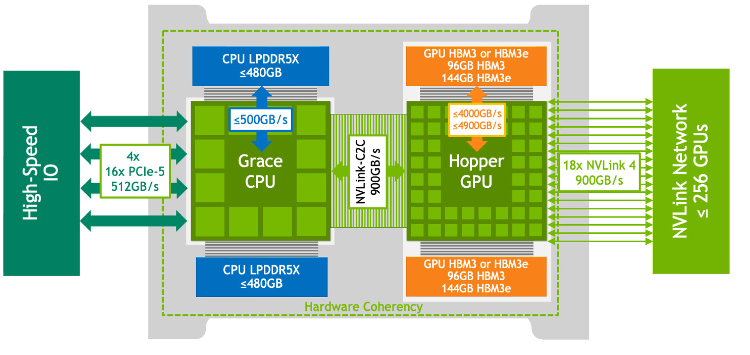
Figure: NVIDIA GH200 reference architecture. Source: NVIDIA GH200 datasheet.
Coherent Memory for Larger Workloads
NVLink-C2C provides coherent CPU–GPU memory access, shared address translation, and atomic operations.
NVIDIA describes up to 624 GB of combined accessible memory per Superchip in a configuration with 480 GB of LPDDR5X CPU memory and 144 GB of HBM3e GPU memory. See the NVIDIA GH200 architecture whitepaper for further details.
CPU LPDDR5X and GPU HBM3e remain separate memories with different bandwidths. Data placement affects performance.
The 900 GB/s NVLink-C2C figure describes the CPU–GPU interconnect within a Superchip.
Memory Access across Connected Superchips
In supported reference configurations, GPUs can also access peer memory through GPU-to-GPU NVLink. These paths have different latency and bandwidth.
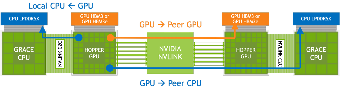
Figure: Memory access across connected Grace Hopper Superchips. Source: NVIDIA GH200 architecture whitepaper.
Performance Highlights
The NVIDIA GH200 datasheet lists the following peak GPU arithmetic rates per GH200. Precision and execution mode matter: Tensor Core figures apply to supported matrix operations and should not be interpreted as general-purpose CPU or GPU application throughput.
| Arithmetic mode | Peak per GH200 GPU |
|---|---|
| FP64 | 34 TFLOPS |
| FP64 Tensor Core | 67 TFLOPS |
| FP32 | 67 TFLOPS |
| FP16 / BF16 Tensor Core, dense | 990 TFLOPS |
| FP8 Tensor Core, dense | 1,979 TFLOPS |
FP8 with supported sparsity reaches a theoretical 3,958 TFLOPS. All figures are vendor peaks, not measured application performance.